NVIDIA NVLink Fusion and NVHBM: The New Plumbing of Custom AI Silicon
NVIDIA just opened up its high-end plumbing to competitors and hyperscalers, rewriting the rules for custom AI chip design....

Building custom silicon is a brutal exercise in compromise. Every millimeter of a silicon package is fiercely contested real estate, a brutal zero-sum game where compute logic constantly fights memory stacks, thermal limits. Also, power delivery networks for physical space. Should you want more processing cores, you have to starve the memory. If you want blistering data transfer speeds, you sacrifice precious die area that could otherwise be used for raw compute. Hyperscalers pouring billions into custom AI accelerators, or XPUs, have hit a brick wall trying to balance these constraints while chasing models that grow larger by the day.
Enter NVIDIA NVLink Fusion. It is a calculated, pragmatic play from a company that usually prefers to keep everyone trapped inside its proprietary walled garden. By licensing its scale-up and scale-out architecture alongside custom NVHBM base-die technology, NVIDIA is letting hyperscalers plug their own proprietary compute silicon directly into the MGX rack infrastructure. They are handing over the blueprints to the plumbing. Why? Because as data centers balloon to rack-scale monsters running complex agentic reasoning workloads, controlling the interconnection standard is infinitely more profitable than fighting every custom chip designer in court.
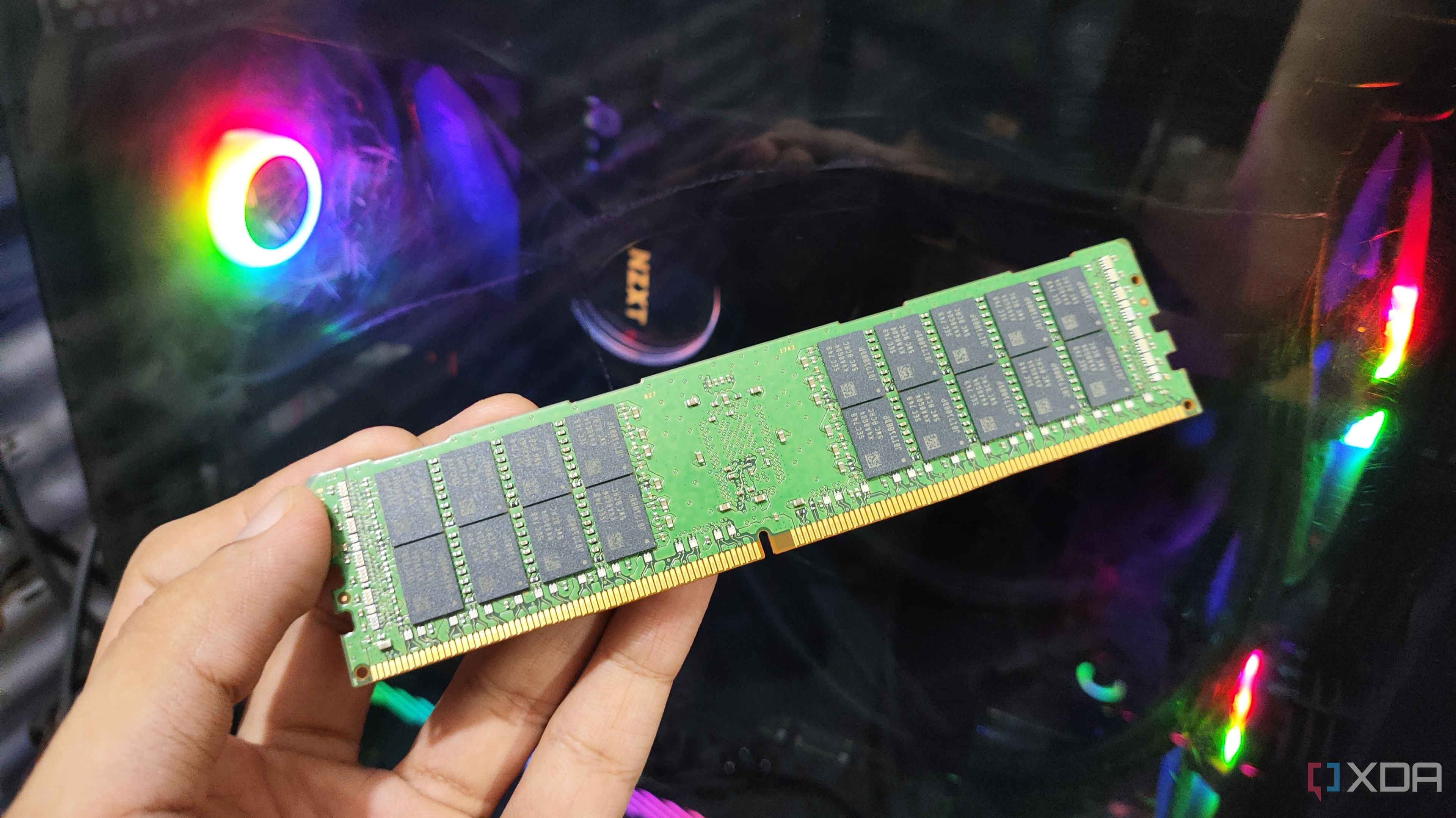
The engineering specs behind NVHBM — oddly — are genuinely impressive, cutting through the usual promo fluff with hard physics. This by collaborating directly with memory vendors on a custom base-die! Sounds familiar? They've squeezed out roughly 30 percent more bandwidth than standard HBM4e while reclaiming up to 25 percent more die area for actual compute logic. I guess, fifteen percent lower power consumption might sound modest (to be fair) on paper, but multiply those watts across tens of thousands of accelerators humming away in a modern data center. And you're looking at millions of dollars saved in cooling bills alone. Qualification bottlenecks have historically killed custom chip projects before they ever left the fab. So getting pre-validated memory setup is a massive shortcut for teams trying to tape out quickly.
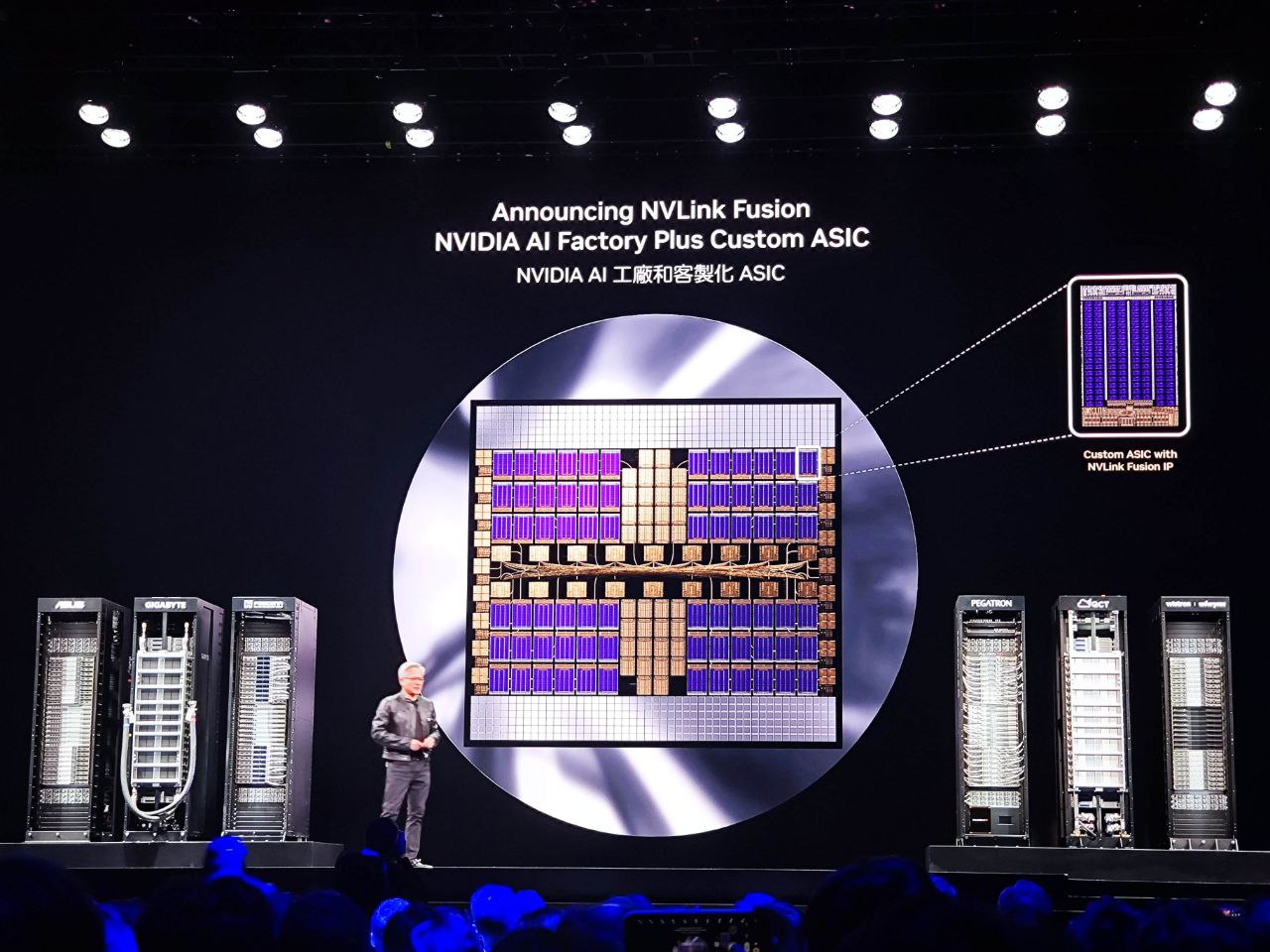
Of course, there is no free lunch in hardware. Hitching your custom accelerator roadmap to NVIDIA's interconnect ecosystem means playing by their rules, even if you are building the core processing logic yourself. You avoid the nightmare of designing custom memory interfaces from scratch. However, you also cement their infrastructure as the default gravity well of the modern data center. It is a brilliant tactical retreat that secures their hardware monopoly at the networking and memory layer. It is a brilliant tactical retreat that secures their hardware monopoly at the networking and memory layer.
builders care about throughput, latency — and whether their KV cache can keep up with real-time inference demands. The If NVLink Fusion and NVHBM actually deliver these gains without locking a team into a monolithic GPU purchase! It changes the math for custom silicon. At the same time, the bottom line? Actually. We're watching the base layer evolve in real-time — and the teams that master these packaging constraints will own the next decade of compute.